Adam Zewe | MIT News Office
August 12, 2022
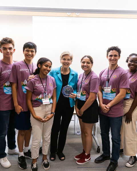
To celebrate the passage of the CHIPS and Science Act of 2022 — which authorizes major funding increases for scientific research and provides about $52 billion for U.S. semiconductor research, development, and manufacturing — Sen. Elizabeth Warren paid a visit to MIT’s state-of-the-art facility for nanoscale science and engineering on Wednesday.
She arrived at MIT.nano, a shared 214,000-square-foot nanoscale research center located in the heart of campus, one day after President Joe Biden signed the bipartisan measure into law. The act aims to help the U.S. reassert its leadership in microelectronics research, development, and manufacturing, while also expanding the semiconductor workforce. It also authorizes significantly expanded funding for the National Science Foundation, where a new Technology, Innovation, Partnerships Directorate will be established.
“I believe our job in Washington is to build for the future,” Warren said, addressing a roundtable of university leaders after she toured the MIT.nano facility. “I am delighted about $52 billion that is going into chips, that is going into domestic manufacturing, that is going into strengthening our supply chains. But keep in mind … we’ve [also got billions] going directly into increasing the budget of the National Science Foundation. That has the potential to be transformative.”
Complete article from MIT News.
Explore
MIT Engineers Advance Toward a Fault-tolerant Quantum Computer
Adam Zewe | MIT News
Researchers achieved a type of coupling between artificial atoms and photons that could enable readout and processing of quantum information in a few nanoseconds.
The Road to Gate-All-Around CMOS
Monday, April 14, 2025 | 10:00 AM to 11:00 AM
In-Person
Haus Room (36-428)
50 Vassar Street Cambridge, MA
2025 MIT AI Hardware Program Annual Symposium
Monday, March 31, 2025 | 10:00 AM - 3:30 PM ET
Multiple Speakers


