January 30, 2024
MIT and Applied Materials, Inc., announced an agreement today that, together with a grant to MIT from the Northeast Microelectronics Coalition (NEMC) Hub, commits more than $40 million of estimated private and public investment to add advanced nano-fabrication equipment and capabilities to MIT.nano, the Institute’s center for nanoscale science and engineering. The collaboration will create a unique open-access site in the United States that supports research and development at industry-compatible scale using the same equipment found in high-volume production fabs to accelerate advances in silicon and compound semiconductors, power electronics, optical computing, analog devices, and other critical technologies.
The equipment and related funding and in-kind support provided by Applied Materials will significantly enhance MIT.nano’s existing capabilities to fabricate up to 200-millimeter (8-inch) wafers, a size essential to industry prototyping and production of semiconductors used in a broad range of markets including consumer electronics, automotive, industrial automation, clean energy, and more. Positioned to fill the gap between academic experimentation and commercialization, the equipment will help establish a bridge connecting early-stage innovation to industry pathways to the marketplace.
Complete article from MIT News.
Explore
MIT Engineers Advance Toward a Fault-tolerant Quantum Computer
Adam Zewe | MIT News
Researchers achieved a type of coupling between artificial atoms and photons that could enable readout and processing of quantum information in a few nanoseconds.
III-Nitride Ferroelectrics for Integrated Low-Power and Extreme-Environment Memory
Monday, May 5, 2025 | 4:00 - 5:00pm ET
Hybrid
Zoom & MIT Campus
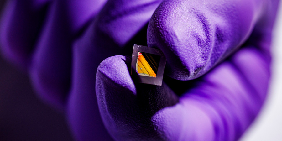
New Electronic “skin” could Enable Lightweight Night-vision Glasses
Jennifer Chu | MIT News
MIT engineers developed ultrathin electronic films that sense heat and other signals, and could reduce the bulk of conventional goggles and scopes.