Explore
III-Nitride Ferroelectrics for Integrated Low-Power and Extreme-Environment Memory
Monday, May 5, 2025 | 4:00 - 5:00pm ET
Hybrid
Zoom & MIT Campus
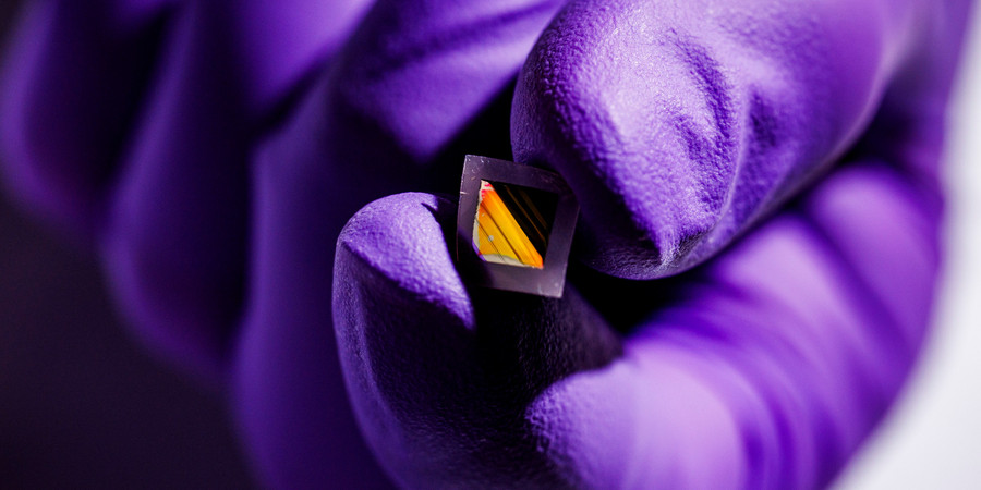
New Electronic “skin” could Enable Lightweight Night-vision Glasses
Jennifer Chu | MIT News
MIT engineers developed ultrathin electronic films that sense heat and other signals, and could reduce the bulk of conventional goggles and scopes.
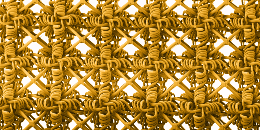
MIT Engineers Print Synthetic “Metamaterials” that are Both Strong and Stretchy
Jennifer Chu | MIT News
A new method could enable stretchable ceramics, glass, and metals, for tear-proof textiles or stretchy semiconductors.