Jennifer Chu | MIT News Office
January 18, 2023
True to Moore’s Law, the number of transistors on a microchip has doubled every year since the 1960s. But this trajectory is predicted to soon plateau because silicon — the backbone of modern transistors — loses its electrical properties once devices made from this material dip below a certain size.
Enter 2D materials — delicate, two-dimensional sheets of perfect crystals that are as thin as a single atom. At the scale of nanometers, 2D materials can conduct electrons far more efficiently than silicon. The search for next-generation transistor materials therefore has focused on 2D materials as potential successors to silicon.
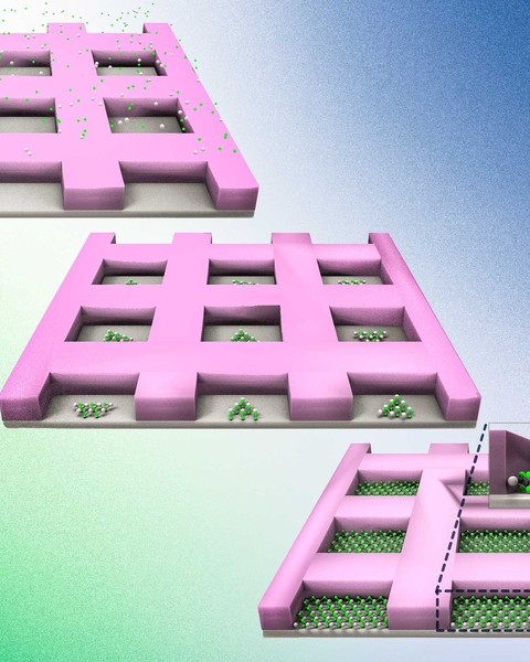
But before the electronics industry can transition to 2D materials, scientists have to first find a way to engineer the materials on industry-standard silicon wafers while preserving their perfect crystalline form. And MIT engineers may now have a solution.
Complete article from MIT News.
Explore
III-Nitride Ferroelectrics for Integrated Low-Power and Extreme-Environment Memory
Monday, May 5, 2025 | 4:00 - 5:00pm ET
Hybrid
Zoom & MIT Campus
New Electronic “skin” could Enable Lightweight Night-vision Glasses
Jennifer Chu | MIT News
MIT engineers developed ultrathin electronic films that sense heat and other signals, and could reduce the bulk of conventional goggles and scopes.
MIT Engineers Print Synthetic “Metamaterials” that are Both Strong and Stretchy
Jennifer Chu | MIT News
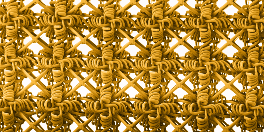
A new method could enable stretchable ceramics, glass, and metals, for tear-proof textiles or stretchy semiconductors.


