December 8, 2023
Two-dimensional materials, which are only a few atoms thick, can exhibit some incredible properties, such as the ability to carry electric charge extremely efficiently, which could boost the performance of next-generation electronic devices.
But integrating 2D materials into devices and systems like computer chips is notoriously difficult. These ultrathin structures can be damaged by conventional fabrication techniques, which often rely on the use of chemicals, high temperatures, or destructive processes like etching.
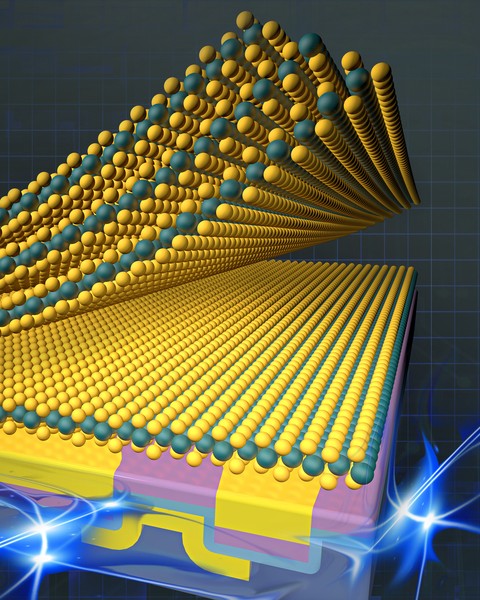
To overcome this challenge, researchers from MIT and elsewhere have developed a new technique to integrate 2D materials into devices in a single step while keeping the surfaces of the materials and the resulting interfaces pristine and free from defects.
Their method relies on engineering surface forces available at the nanoscale to allow the 2D material to be physically stacked onto other prebuilt device layers. Because the 2D material remains undamaged, the researchers can take full advantage of its unique optical and electrical properties.
Complete article from MIT News.
Explore
MIT Engineers Advance Toward a Fault-tolerant Quantum Computer
Adam Zewe | MIT News
Researchers achieved a type of coupling between artificial atoms and photons that could enable readout and processing of quantum information in a few nanoseconds.
III-Nitride Ferroelectrics for Integrated Low-Power and Extreme-Environment Memory
Monday, May 5, 2025 | 4:00 - 5:00pm ET
Hybrid
Zoom & MIT Campus
New Electronic “skin” could Enable Lightweight Night-vision Glasses
Jennifer Chu | MIT News
MIT engineers developed ultrathin electronic films that sense heat and other signals, and could reduce the bulk of conventional goggles and scopes.


