Study Unlocks Nanoscale Secrets for Designing Next-generation Solar Cells
David L. Chandler | MIT News
The work will help researchers tune surface properties of perovskites, a promising alternative and supplement to silicon, for more efficient photovoltaics.

Magnetic Imaging with NV Centers in Diamond
Tuesday, March 5, 2024 | 11:00am - 12:00pm ET
Virtual
Speaker: Samuel Karlson, MIT
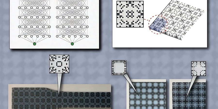
Using AI to Discover Stiff and Tough Microstructures
Rachel Gordon | MIT CSAIL
Innovative AI system from MIT CSAIL melds simulations and physical testing to forge materials with newfound durability and flexibility for diverse engineering uses.

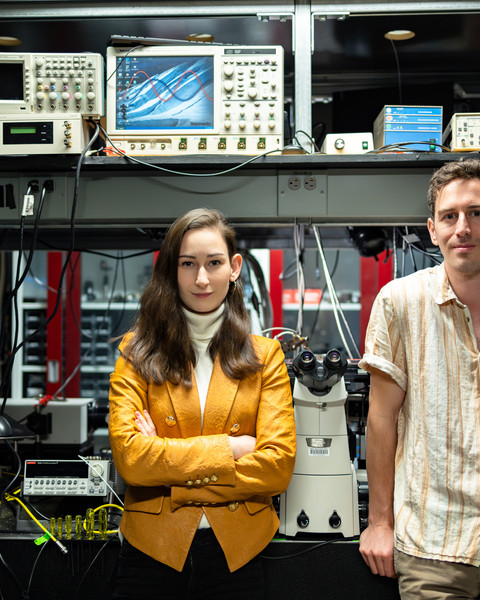
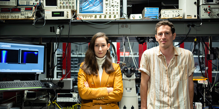
Technique Could Improve the Sensitivity of Quantum Sensing Devices
Adam Zewe | MIT News
New method lets researchers identify and control larger numbers of atomic-scale defects, to build a bigger system of qubits.

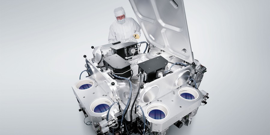
MIT, Applied Materials, and the Northeast Microelectronics Coalition Hub to bring 200mm Advanced Research Capabilities to MIT.nano
MIT.nano
State-of-the-art toolset will bridge academic innovations and industry pathways to scale for semiconductors, microelectronics, and other critical technologies.
New MIT.nano Equipment to Accelerate Innovation in “Tough Tech” Sectors
Zach Winn | MIT News
The advanced fabrication tools will enable the next generation of microelectronics and microsystems while bridging the gap from the lab to commercialization.

Closing the Design-to-Manufacturing Gap for Optical Devices
Adam Zewe | MIT News
A new method enables optical devices that more closely match their design specifications, boosting accuracy and efficiency.
MIT Group Releases White Papers on Governance of AI
Peter Dizikes | MIT News
MIT has released a new set of policy papers about the governance of artificial intelligence, with aims to help policymakers create better oversight of AI in society.
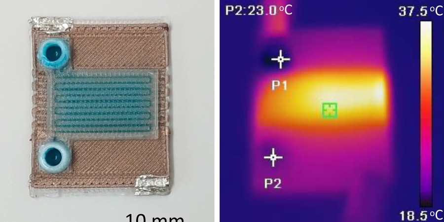
Scientists 3D Print Self-heating Microfluidic Devices
Adam Zewe | MIT News
The one-step fabrication process rapidly produces miniature chemical reactors that could be used to detect diseases or analyze substances.
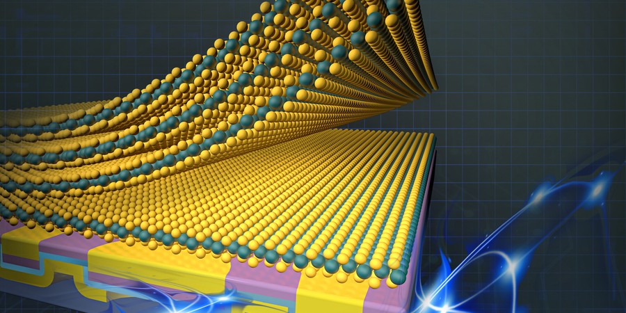
Researchers Safely Integrate Fragile 2D Materials into Devices
Adam Zewe | MIT News
The advance opens a path to next-generation devices with unique optical and electronic properties.