

Life is short, so aim high
Michaela Jarvis | MIT News
Professor Rafael Jaramillo relishes the challenge of developing new, environmentally beneficial semiconductor materials.
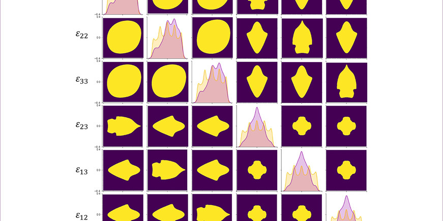
A first-ever Complete Map for Elastic Strain Engineering
Peter Reuell | Department of Nuclear Science and Engineering
New research by a team of MIT engineers offers a guide for fine-tuning specific material properties.
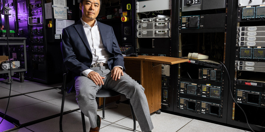
Pushing Material Boundaries for Better Electronics
Jennifer Chu | MIT News
Associate Professor Jeehwan Kim is exploring systems that could take over where silicon leaves off.
Shaping a Soft Future
Wednesday, March 13, 2024 | 12:00 - 1:00pm ET
In-person
Allen Room (36-462)
50 Vassar Street Cambridge, MA
Study Unlocks Nanoscale Secrets for Designing Next-generation Solar Cells
David L. Chandler | MIT News
The work will help researchers tune surface properties of perovskites, a promising alternative and supplement to silicon, for more efficient photovoltaics.
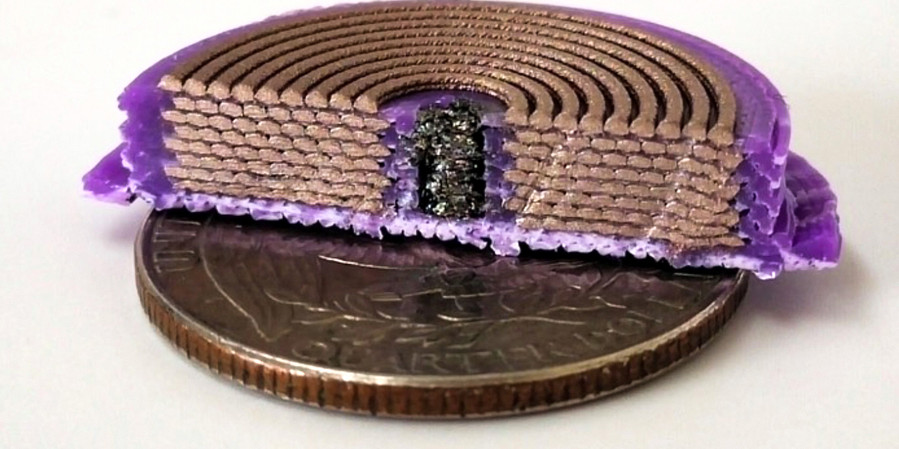
MIT Engineers 3D Print the Electromagnets at the Heart of Many Electronics
Adam Zewe | MIT News
The printed solenoids could enable electronics that cost less and are easier to manufacture — on Earth or in space.

Electrons Become Fractions of Themselves in Graphene, Study Finds
Jennifer Chu | MIT News
An exotic electronic state observed by MIT physicists could enable more robust forms of quantum computing.
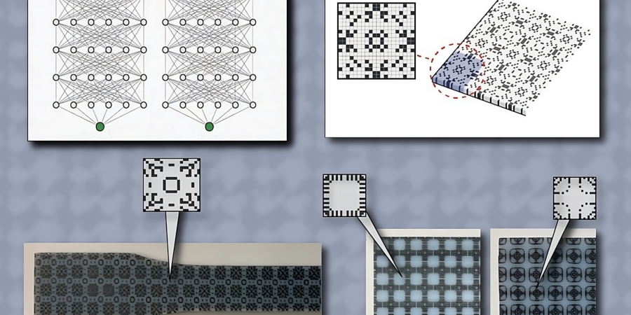
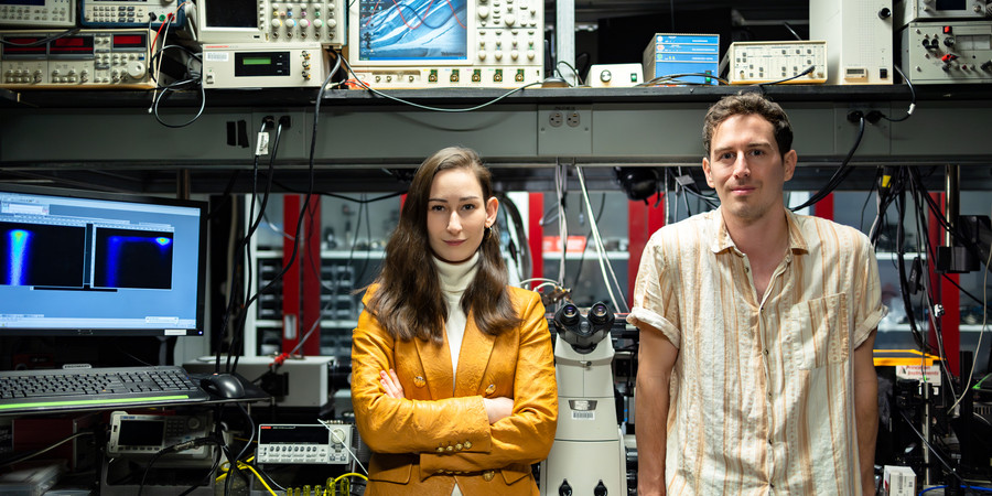
Using AI to Discover Stiff and Tough Microstructures
Rachel Gordon | MIT CSAIL
Innovative AI system from MIT CSAIL melds simulations and physical testing to forge materials with newfound durability and flexibility for diverse engineering uses.

MIT, Applied Materials, and the Northeast Microelectronics Coalition Hub to bring 200mm Advanced Research Capabilities to MIT.nano
MIT.nano
State-of-the-art toolset will bridge academic innovations and industry pathways to scale for semiconductors, microelectronics, and other critical technologies.
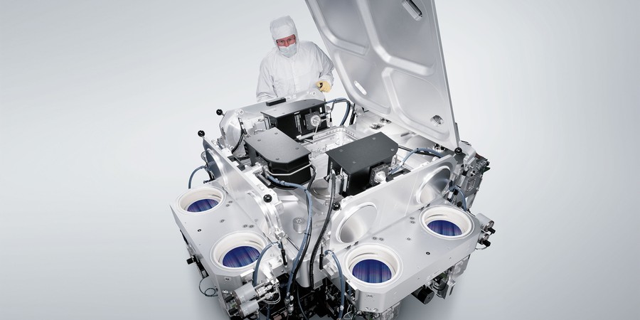
New MIT.nano Equipment to Accelerate Innovation in “Tough Tech” Sectors
Zach Winn | MIT News
The advanced fabrication tools will enable the next generation of microelectronics and microsystems while bridging the gap from the lab to commercialization.