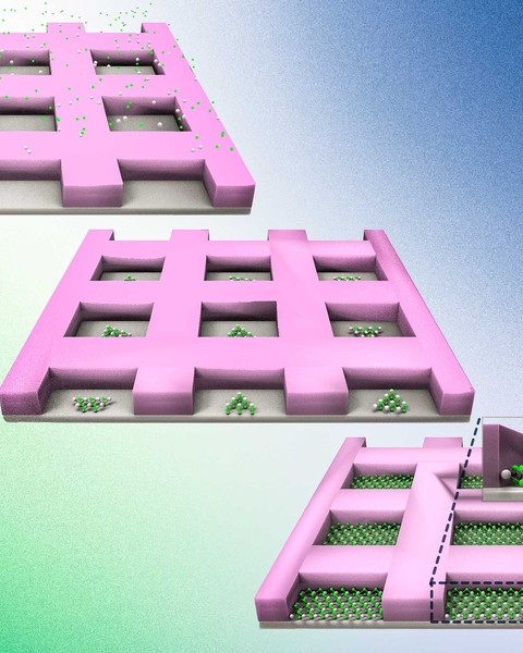
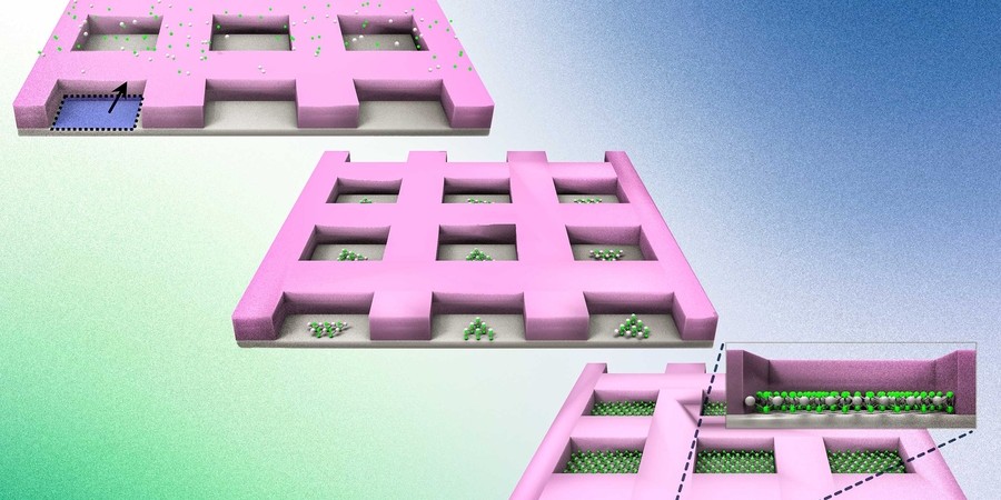
MIT engineers grow “perfect” atom-thin materials on industrial silicon wafers
Jennifer Chu | MIT News Office
New technique could allow chip manufacturers to produce next-generation transistors based on materials other than silicon.

Ferroelectric Memories at Last
Wednesday, March 15, 2023 | 1:00 - 2:00pm ET
Speaker: Beatriz Noheda

The Future of Semiconductor Manufacturing
Friday, March 17, 2023 | 3:00 - 4:00pm ET,
MIT Building E51-115, Wong Auditorium, Tang Center
Speaker: Pat Gelsinger, Intel

Advances in Additive Manufacturing
Thursday, February 16, 2023 | 10:00am - 12:00pm ET
Multiple Speakers

Chips & Innovation: A New Era
Wednesday, January 18, 2023 | 3:00 - 4:00pm ET,
MIT Building 34-401A, Grier Room A
Speaker: Ahmad Bahai, Texas Instruments
Manufacturing a Cleaner Future
Mary Beth Gallagher | Department of Mechanical Engineering
Startups founded by mechanical engineers are at the forefront of developing solutions to mitigate the environmental impact of manufacturing.
The US Can Shape the Future of Semiconductors if Congress Thinks Ahead
Rafael Reif | The Hill, Opinion Contributor
Spurred by strained supply chains, growing concerns about China, and the landmark CHIPS and Science Act Congress enacted last summer, U.S. semiconductor manufacturing seems poised for a renaissance.
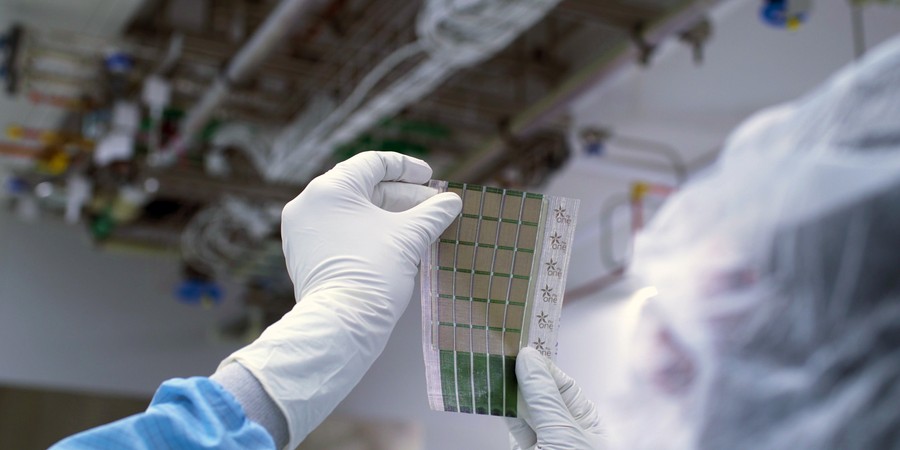
Paper-thin Solar Cell Can Turn any Surface into a Power Source
Adam Zewe | MIT News Office
Researchers develop a scalable fabrication technique to produce ultrathin, lightweight solar cells that can be seamlessly added to any surface.

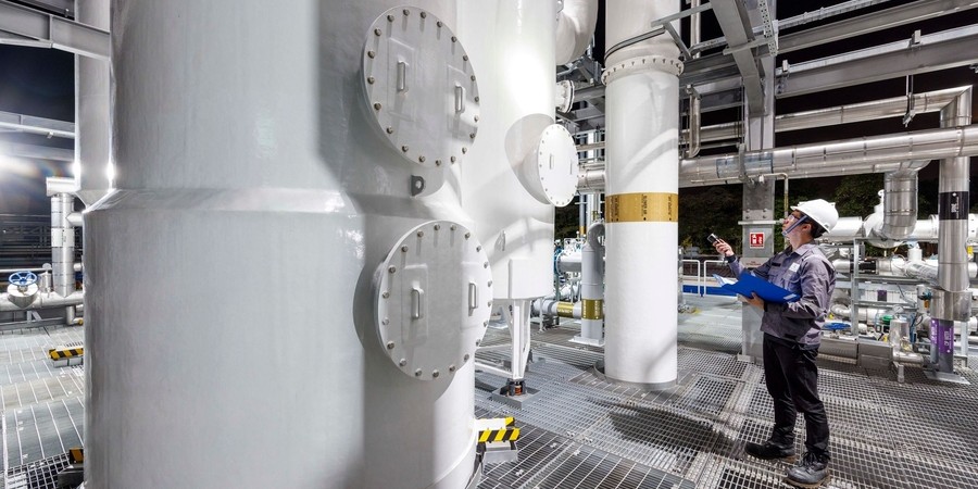
3 Questions: Blue Hydrogen and the World’s Energy Systems
Turner Jackson | MIT Energy Initiative
Research Scientist Emre Gençer describes natural gas–based hydrogen production with carbon capture and storage, and the role hydrogen will play in decarbonizing our energy systems.

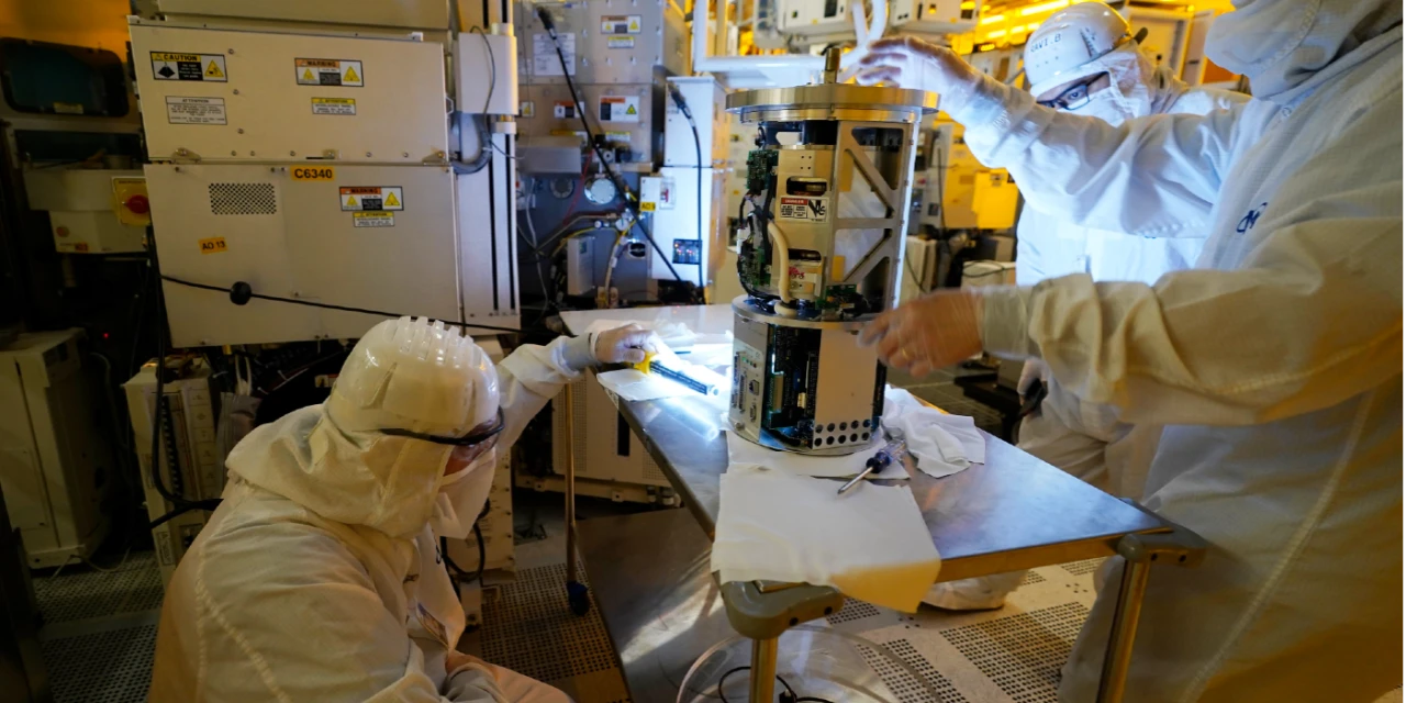
MIT.nano Adds New Instruments to Create and Analyze at the Nanoscale
MIT.nano
MIT.nano has added several new instruments, expanding the facilities’ capabilities at the nanoscale. These new tools can accommodate samples from small pieces up to 200 mm wafers.